For more than half a decade, China has quietly but relentlessly pursued one objective that sits at the heart of its technological and geopolitical ambitions: complete independence in advanced semiconductor manufacturing. That long-running effort now appears to have reached a critical milestone.
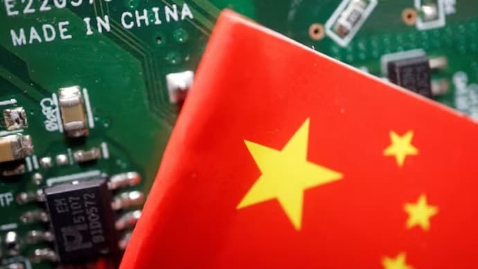
According to information obtained by Reuters, Chinese scientists have built what Washington and its allies have spent years trying to prevent—a working prototype of a machine capable of producing the world’s most advanced semiconductor chips. These chips power everything from smartphones and Artificial Intelligence systems to advanced weapons platforms that underpin Western military superiority.
The prototype has been assembled inside a heavily secured research facility in Shenzhen, one of China’s most important technology hubs. Sources familiar with the matter say the project represents a turning point in the global semiconductor race.
The massive machine, which occupies nearly an entire factory floor, was completed in early 2025 and is currently undergoing intensive testing. Two people with direct knowledge of the initiative told Reuters that the system was developed by a group of former engineers from ASML, the Dutch company that holds a near-monopoly over extreme ultraviolet (EUV) lithography technology.
These engineers reportedly reverse-engineered ASML’s EUV machines—an extraordinary technical challenge that has long been considered beyond China’s reach.
At the center of today’s technology cold war lies EUV lithography. These machines use highly focused ultraviolet laser beams to etch circuits onto silicon wafers at scales thousands of times thinner than a human hair. The smaller the circuits, the more powerful and efficient the chips—making EUV technology indispensable for cutting-edge AI processors.
Until now, EUV has remained an exclusive Western capability.
People familiar with the Shenzhen project say China’s prototype is already generating powerful ultraviolet light, a key technical hurdle. However, it has not yet produced fully functional chips that meet commercial standards.
In April, ASML CEO Christophe Fouquet publicly stated that China would need “many, many years” to develop comparable EUV technology. Yet the existence of this prototype—revealed for the first time by Reuters—suggests Beijing may be far closer to semiconductor independence than most analysts previously believed.
That said, significant challenges remain. Replicating the ultra-precise optical systems manufactured by Western suppliers continues to be one of China’s biggest obstacles.
According to two sources, China has been able to assemble the prototype by sourcing components from older ASML machines available on secondary markets. The government’s internal target is to produce working chips on this platform by 2028.
Insiders involved in the project, however, caution that a more realistic timeline points to 2030. Even that would be well ahead of earlier predictions that China would need at least a decade to close the gap with the West.
Chinese authorities did not respond to multiple requests for comment.
Although Beijing has openly declared its ambition to dominate semiconductor manufacturing, sources say the Shenzhen EUV effort has been conducted largely in secrecy. The program is reportedly classified under National Security protocols.
Official Chinese media indicate that Ding Xuexiang—a senior Communist Party leader and close ally of President Xi Jinping—oversees the initiative through the Central Science and Technology Commission.
Huawei, China’s flagship technology giant, plays a pivotal role. According to multiple sources, the company has helped coordinate a nationwide network of private firms, state-owned enterprises, and government research institutions employing thousands of scientists and engineers.
Several insiders have compared the scale and secrecy of the initiative to China’s own version of the United States’ Manhattan Project, which developed the atomic bomb during World War II.
“The ultimate goal is for China to manufacture advanced chips entirely on domestically built machines,” one source said. “Beijing wants the United States completely removed from its semiconductor supply chains.”
Huawei, China’s State Council, the Ministry of Industry and Information Technology, and the Chinese Embassy in Washington declined to comment.
At present, ASML remains the only company in the world that has successfully mastered EUV lithography. Based in Veldhoven, the Netherlands, its machines—each costing roughly $250 million—are essential for producing the most advanced chips designed by firms like Nvidia and AMD and manufactured by TSMC, Intel, and samsung.
ASML developed its first EUV prototype in 2001. The company has said it took nearly two decades and billions of euros in research and development before commercial production became possible in 2019.
“It’s understandable that others want to replicate our technology, but doing so is extraordinarily complex,” ASML said in a statement. Its EUV systems are currently supplied only to U.S. allies such as Taiwan, South Korea, and Japan.
Beginning in 2018, Washington pressured the Dutch government to block EUV exports to China. Those efforts intensified in 2022 when the Biden administration imposed sweeping export controls aimed at cutting off China’s access to advanced chipmaking technology.
ASML has confirmed that it has never sold an EUV machine to a Chinese customer.
To ensure China remains at least one generation behind in chip manufacturing, U.S. restrictions also targeted older deep ultraviolet (DUV) systems used to make less advanced chips, including those used by Huawei.
The U.S. State Department has said successive administrations have strengthened enforcement of export controls and are working with allies to “close loopholes as technology advances.”
Meanwhile, the Netherlands has introduced new regulations requiring background screenings at research institutions to prevent sensitive technology from being accessed by individuals deemed vulnerable to pressure or malicious intent.
According to sources, these export restrictions severely slowed Huawei’s advanced chip production and delayed China’s progress toward self-sufficiency.
Because of the project’s classified nature, all sources spoke on condition of anonymity.
The ‘Manhattan Project’ Inside China
One experienced Chinese engineer recruited from ASML reportedly discovered that his generous signing bonus came with a surprise: an identity card issued under a false name.
Once inside the facility, he recognized other former ASML colleagues—also operating under aliases. They were instructed to use these assumed identities at all times to maintain secrecy.
Multiple sources independently confirmed that fake IDs were standard practice within the secure compound.
The message was unambiguous: the project was classified under national security, and no one outside the facility was allowed to know what was being built—or who was building it.
The core team consists largely of retired or recently departed Chinese-born ASML scientists and engineers. Their deep technical expertise and lack of post-employment restrictions made them especially valuable recruits.
Huawei recruiters have reportedly been approaching Chinese ASML employees in Europe since at least 2020.
ASML’s ability to track former employees is limited by European privacy laws, and enforcing non-disclosure agreements across borders has proven difficult.
In 2019, ASML won an $845 million legal verdict against a former Chinese engineer accused of stealing trade secrets. The individual later declared bankruptcy and continues to operate in Beijing with reported government backing.
ASML says it “vigilantly protects” its intellectual property and restricts access to EUV expertise even within its own organization.
Dutch intelligence agencies have warned that China has used extensive espionage programs, including recruiting Western scientists, to acquire advanced technology.
Sources say the Shenzhen breakthrough would have been nearly impossible without the insider knowledge of former ASML engineers.
In 2019, China launched an aggressive overseas recruitment campaign, offering multimillion-yuan incentives and housing benefits to semiconductor experts.
One notable recruit was Lin Nan, former head of light source technology at ASML. Patent records show his team in Shanghai filed eight EUV-related patents within just 18 months.
Inside China’s EUV Fabrication Facility
ASML’s most advanced EUV machines weigh around 180 tons and are roughly the size of a school bus. China’s prototype is reportedly even larger, built to increase power after earlier design attempts failed.
While less refined than ASML’s systems, the Chinese machine is functional enough for testing, sources say.
A major bottleneck remains optics. German firm Carl Zeiss AG, a key ASML supplier, produces mirrors so precise they take months to manufacture. Replicating that capability has proven extremely difficult.
EUV machines generate plasma at temperatures nearing 200,000 degrees Celsius by firing lasers at molten tin tens of thousands of times per second.
Chinese research institutions have made progress on domestic alternatives, including breakthroughs by the Changchun Institute of Optics.
China has also sourced parts through secondhand markets and dismantled older ASML machines. Networks of intermediaries are sometimes used to obscure final buyers.
According to sources, the prototype incorporates restricted components originally manufactured by Japan’s Nikon and Canon.
Older lithography equipment has continued to appear in Chinese auctions, including listings as recent as October 2025.
Roughly 100 newly graduated engineers are reportedly working full-time on reverse-engineering EUV and DUV components, with their work constantly monitored and incentivized through performance bonuses.
Huawei Engineers Sleeping On-Site
Although the Chinese government oversees the project, Huawei is embedded across the entire supply chain—from chip design and equipment to manufacturing and product integration.
Sources say Huawei founder Ren Zhengfei personally briefs senior Chinese leaders on progress.
Since being placed on a U.S. entity list in 2019, Huawei has faced sweeping restrictions—but that pressure appears to have intensified its domestic innovation drive.
Engineers assigned to sensitive semiconductor teams reportedly live on-site during the workweek and are prohibited from using personal phones.
To preserve secrecy, teams are isolated from one another. “They don’t know what the other teams are working on,” one source said.
The result is a highly compartmentalized, high-stakes effort—one that could reshape the global balance of power in advanced technology.
For breaking news and live news updates, like us on Facebook or follow us on Twitter and Instagram. Read more on Latest World on thefoxdaily.com.


COMMENTS 0